
2012-5-11
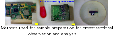
Introduction of mechanical polishing method of pretreatment suitable for sample preparation by argon ion beam equipment.

Cross-sectional observation by mechanical polishing is a significant technology in the practice of the reliability testing and failure analysis.
Working to improve polishing techniques for more accurate reproduction of the cross section state of mechanical polishing.
For example, is the result of verification of the optimal combination of liquid and buff the finish to be used in the finishing process of polishing.
When used in the finishing process of colloidal silica in the polishing of the cross-section of the electronic components, you can get a good smooth surface by adding hydrogen peroxide, ammonia and water.
Mechanical polishing method of the conventional resin embedding will require craftsmanship. It quickly to deal with sample preparation is difficult. And it is think in the general resin embedding method is Unreasonable to irradiation in the vertical direction fundamentally.
Also Ion beam specimen preparation ,think that diversity a somewhat deficient in the processing of electronic components.
because,the equipment specification will be an inconvenience for a few millimeters in height.
This chapter describes how to use the mechanical polishing of suitable pre-treatment to eliminate inconvenience of sample preparation.
I believe that the potential to achieve unprecedented analysis of electronic components.
Can provide faster and cheaper than a good sample in the polishing machine if it depends on the processing of Ar ion irradiation.
will introduce a examples that improve the convenience of the Ar ion device by smaller and thinner.
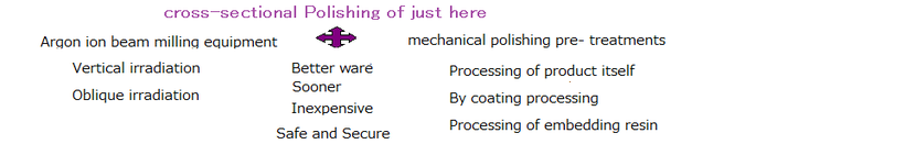
Proposal has provided the following matters: sample preparation by mechanical polishing and argon ion beam processing machine.
1)There are multiple simultaneous machining various ways.
2)Resin coating method for printed circuit assembly is unusual.
3)That does not cause damage to the surface and interface.
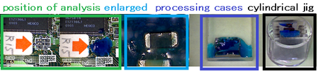
In this section, we introduce the cross-sectional sample preparation in an oblique direction of argon ion irradiation.
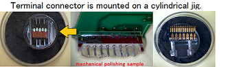
It is a state attached to the jig after the mechanical polishing. Is a cylindrical jig for mounting to the equipment of Ar ions.
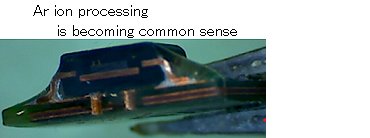
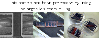
This sample has been processed by using an argon ion beam milling. Resin embedding method and the method is nearly equivalent.
Surface finish machining by argon ion, there is no difference between the embedding resin and the resin coating.
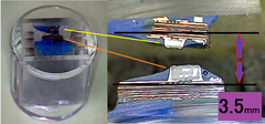
cross-sectional Processing of a flat cable IDC connector terminal shown in the photo is a unique way.
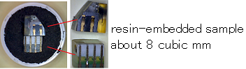
Sample preparation by mechanical polishing of small precision parts.
Resin-embedded samples of about 8 cubic mm square.
Bonding wire junction cross section is example of simultaneous machining of two pieces semiconductors.
It is multiple simultaneous processing of different varieties.
Resistor and capacitor is an example of simultaneous processing of two pieces.
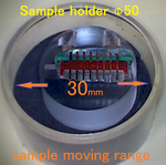
Devised jig Mounting to the device of Ar ions, the range of the irradiation can be more than three times.
The sample will be in the range of irradiation of 15mm by moving from side to side.
In this section, we introduce the cross-sectional sample preparation in an vertical direction of argon ion irradiation.

Photo after removal of mount components.
To prepare a sample of the height of a few mm, it is possible to polishing one side of the surface mount components.
Base material was thinned to 0.5mm from the processing of 1.6 mm.
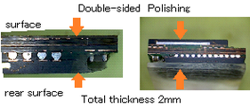
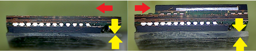
Some products of the printed circuit assembly may exceed the height of 14 mm. The total thickness of the PCB is an example of processing to a thickness of 2mm in 14 mm.

must be processed into a rectangular shape if need an argon ion processing.
There was an irrational thing that requires a re-processing at the variation in the processing.
It had to be reworked to a thickness of 2mm with a rectangle than cylindrical.
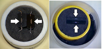
The photograph is a sample of the resin coating method is processed by mechanical polishing.
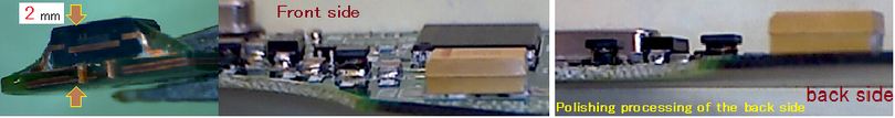
The height of the printed circuit assembly has exceeded 12 mm in a state of irregularity.
Point of the photo will be the PCB of 2mm thickness by remove a portion of the PCB surface mount components of the height of 12mm.

Think a high possibility of analysis by Auger electron spectroscopy.
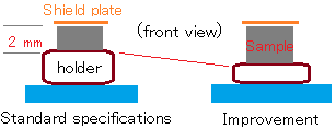
The length of the dimensions that protrude from the argon ion shielding plate is important.
The center of the wire bond, can handle protruding from the shield plate of about 100μ.
This state of the LED lamp can be a vertical irradiation.

Must be processed into a 0.5 mm to 1.6mm thickness of the base material in order to secure a sample of 5mm height.
Have prepared a 3mm height because it exceeds the specifications of the of Ar ions.
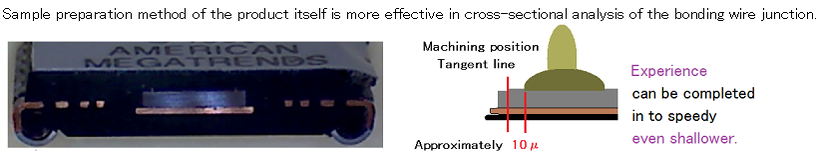
Mechanical polishing process close to the tangent is the just the way here.
Processing and machine processing of Ar ion is feel a need a considerable amount of time.
can reduce the machining time of bonding cross section.
Gas consumption and shield plate consumable Is reduced.
Describes the new ways to take advantage of this section, the device.
proposal to company certain.
Schematic diagram of the improvement of the sample holder is the contents of the proposal offer.
Mounting of the sample is a little technique is required.
In the standard specification of the argon ion will have no inconvenience in the analysis of printed circuit assembly?
Analysis, you will be able to argon ion milling processing of electronic components mounted on the PCB that was not possible so far.
Proposal is a Modify in the vertical irradiation from oblique irradiation of the device.
In other words, you can Available both the vertical irradiation and oblique irradiation by use of the jig.
【Considerations for the processing of an Ar ion beam vertical direction】
Argon ion beam sample preparation device think is somewhat lacking the diversity to process electronic components.
That device can not be irradiated with an argon ion beam from the top of the sample depending on the Height of the sample.
will need to lower the sample height as much as possible.
Think it is necessary to consider the review of resin embedding method for processing if want to depend on the Ar ion.
will introduce the main ones obtained in the result of careful study currently in progress.
Vertical direction can be irradiated with high sample sizes.
1)Prior confirmation was able to gain a better understanding of equipment manufacturers.
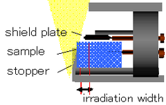
2)Shield plate moves back and forth, the sample is fixed by the stopper.
3)Samples can mount the Min"H7 × W35 × D15mm size.Max"H21×W10×D15mm
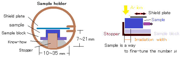

Its status shows that the Incorporate of stopper and sample.
1
A really long time, Thank you very much for your attention.
I think it is bad writing.
My English is poor. If you have any questions, Please feel free to contact us.
Finally,Creating Web Sites with the English translation software from the Japanese at service of Google is very pleased.
Once again, thank you to the Google service.